- 您现在的位置:买卖IC网 > Sheet目录1995 > FT7521L6X (Fairchild Semiconductor)IC RESET TIMER 7.5SEC 6MICROPAK
2009 Fairchild Semiconductor Corporation
www.fairchildsemi.com
FT7521
Rev. 1.0.7
7
FT7521
—
Re
set
Ti
mer
with
Fi
x
ed
De
lay
and
Rese
t
Pulse
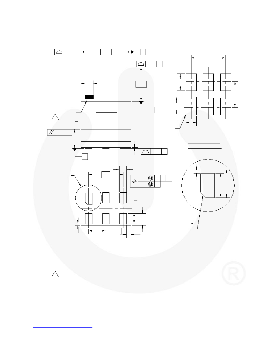
Physical Dimensions
Figure 6.
6-Lead, MicroPak
1.0 x 1.45 mm, JEDEC MO-252
Package drawings are provided as a service to customers considering Fairchild components. Drawings may change in any manner
without notice. Please note the revision and/or date on the drawing and contact a Fairchild Semiconductor representative to verify or
obtain the most recent revision.
Package specifications do not expand the terms of Fairchild’s worldwide terms and conditions, specifically the
warranty therein, which covers Fairchild products.
Always visit
Fairchild Semiconductor’s online packaging area for the most recent package drawings:
2. DIMENSIONS ARE IN MILLIMETERS
1. CONFORMS TO JEDEC STANDARD M0-252 VARIATION UAAD
4. FILENAME AND REVISION: MAC06AREV4
Notes:
3. DRAWING CONFORMS TO ASME Y14.5M-1994
TOP VIEW
RECOMMENED
LAND PATTERN
BOTTOM VIEW
1.45
1.00
A
B
0.05 C
2X
0.55MAX
0.05 C
(0.49)
(1)
(0.75)
(0.52)
(0.30)
6X
1X
6X
PIN 1
DETAIL A
0.075 X 45
CHAMFER
0.25
0.15
0.35
0.25
0.40
0.30
0.5
(0.05)
1.0
5X
DETAIL A
PIN 1 TERMINAL
0.40
0.30
0.45
0.35
0.10
0.00
0.10
C B A
0.05
C
0.05 C
0.05
0.00
5X
6X
(0.13)
4X
6X
PIN 1 IDENTIFIER
(0.254)
5. PIN ONE IDENTIFIER IS 2X LENGTH OF ANY
5
OTHER LINE IN THE MARK CODE LAYOUT.
发布紧急采购,3分钟左右您将得到回复。
相关PDF资料
FT7522L6X
IC RESET TIMER 6-MICROPAK
FT8010UMX
IC RESET TIMER CONF DELAY 10UMLP
FTS125-COO-010.0M
IC GPS BASED TIMING MOD (OCXO)
FTS125-CTV-010.0M
IC GPS BASED TIMING MOD (TCXO)
FTS250-010.0M
IC GPS BASED TIMING MOD (TCXO)
FTS375-010.0M
IC GPS BASED TIMING MOD (OCXO)
HD3-6408-9Z
IC ASMA ADT CMOS 1.25MHZ 24DIP
HI1-565AJD-5
CONV D/A 12BIT 6.7MHZ 24-DIP
相关代理商/技术参数
FT7522
制造商:FAIRCHILD 制造商全称:Fairchild Semiconductor 功能描述:Reset Timer with Fixed Delay and Reset Pulse
FT7522L6X
功能描述:计时器和支持产品 ResetTimer w/ Delay
RoHS:否 制造商:Micrel 类型:Standard 封装 / 箱体:SOT-23 内部定时器数量:1 电源电压-最大:18 V 电源电压-最小:2.7 V 最大功率耗散: 最大工作温度:+ 85 C 最小工作温度:- 40 C 封装:Reel
FT-7600
制造商:GC Electronics 功能描述: 制造商:Winchester Electronics 功能描述:
FT762-03004-043
制造商:Japan Aviation Electronics (JAE) 功能描述:
FT762-03004-055
制造商:Japan Aviation Electronics (JAE) 功能描述:
FT762-03118-044
制造商:Japan Aviation Electronics (JAE) 功能描述:
FT765-03004-054
制造商:Japan Aviation Electronics (JAE) 功能描述:
FT-8
制造商:ITT Interconnect Solutions 功能描述:FT-8 / 995-2000-073 / Tools